

Available 24/7 at
+86 13632816717

What is Ceramic Packaging Chip?
Ceramic packaging plays an important role in modern semiconductor technology, especially in applications that require high reliability, excellent thermal performance, and resistance to harsh environments. Unlike conventional plastic packaging, ceramic packages can withstand higher temperatures and provide strong protection against moisture, chemicals, and mechanical stress. As a result, ceramic packaging is widely used in aerospace, military, automotive, industrial, and other high-reliability electronic systems. In this article, we will explore what ceramic packaging is, why ceramics integrated circuit is important in semiconductors.
What is Ceramic Packaging Chip?
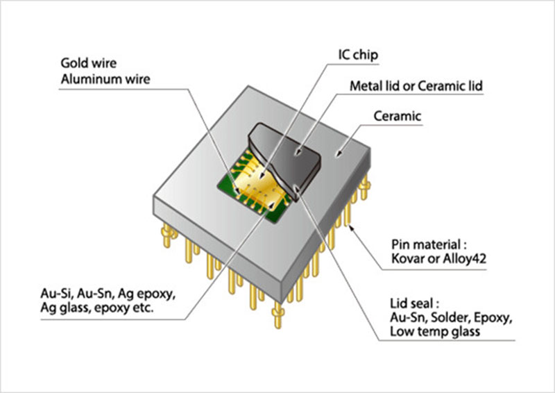
Ceramic packaging is a type of semiconductor and electronic component packaging that uses ceramic materials as the primary package substrate or enclosure.
Common ceramic materials used in electronic packaging include alumina (Al₂O₃), aluminum nitride (AlN), and beryllium oxide (BeO). These materials offer different combinations of thermal conductivity, electrical insulation, mechanical durability, and cost, making them suitable for different applications.
One of the most important advantages of ceramic packaging is its high-temperature performance. Ceramic materials can maintain their structural and electrical properties under temperature conditions that may exceed the practical limits of many plastic packages. This makes ceramic packages particularly suitable for demanding applications such as military and aerospace electronics, automotive systems, industrial equipment, high-power electronics, and high-reliability semiconductor devices.
Ceramic packaging can also provide excellent thermal management. For example, aluminum nitride has relatively high thermal conductivity while maintaining good electrical insulation, allowing heat generated by a chip to be transferred away from the device efficiently. This is especially valuable for high-power or high-performance semiconductor components.
Advantages of Ceramic Packaging in Semiconductors?
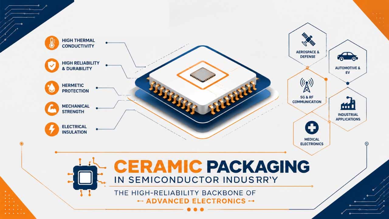
Ceramic packaging is an important technology in semiconductor manufacturing, particularly for electronic components that need to operate reliably under high temperatures, harsh environments, or demanding electrical conditions. It protects the semiconductor die while also providing thermal management, electrical insulation, and reliable connections to external circuits.
1. Superior Thermal Management
Semiconductor devices generate heat during operation, and excessive heat can affect performance, reliability, and service life. Ceramic materials can provide excellent thermal stability and, depending on the material, high thermal conductivity.
For example, aluminum nitride (AlN) combines high thermal conductivity with excellent electrical insulation. This makes it suitable for semiconductor packages that need to dissipate heat efficiently while maintaining electrical isolation.
2. Excellent High-Temperature Performance
Ceramic materials can maintain their mechanical and electrical properties across a wide temperature range. Compared with many conventional plastic packages, ceramic packages are better suited to applications involving continuous operation at elevated temperatures or significant temperature fluctuations.
This high-temperature stability is particularly valuable in automotive, aerospace, military, industrial, and high-power electronic systems.
3. Strong Environmental Protection
A semiconductor package must protect the internal die from external environmental factors. Ceramic packaging offers excellent resistance to:
- Moisture and humidity
- Chemicals and corrosion
- Mechanical stress
- Temperature fluctuations
- Contamination
4. High Electrical Reliability
Ceramic materials generally provide excellent electrical insulation and stable electrical characteristics. A properly designed ceramic package can help maintain signal integrity and electrical isolation while protecting sensitive semiconductor structures.
This makes ceramic packaging suitable for components where stable electrical performance is required over long operating periods.
5. Long-Term Reliability
For many semiconductor applications, reliability is more important than minimizing the initial package cost. Ceramic packages are designed to withstand demanding operating conditions and can provide long service life when properly manufactured and applied.
What are the Different Types of Semiconductor Packaging?
Depending on the application and reliability requirements, semiconductor devices are commonly packaged using metal, ceramic, or plastic materials.
1. Metal Packaging
Metal packaging uses materials such as Kovar, aluminum, copper, and metal alloys to form the package body, lid, or other structural components. Metal has excellent thermal conductivity, mechanical strength, and electromagnetic shielding, allowing it to efficiently transfer heat and protect sensitive circuits from electromagnetic interference (EMI).
Unlike ceramic packaging, which is primarily valued for electrical insulation, metal is electrically conductive. Therefore, metal packages require appropriate insulating structures when electrical isolation is necessary. Metal packaging is commonly used in RF devices, power semiconductors, military electronics, aerospace systems, and other applications requiring strong mechanical protection, heat dissipation, or electromagnetic shielding.
2. Ceramic Packaging
Ceramic packaging uses materials such as alumina (Al₂O₃), aluminum nitride (AlN), and other technical ceramics. Its key characteristics are excellent electrical insulation, high-temperature stability, low moisture permeability, and strong environmental resistance.
Unlike metal packaging, ceramic itself is electrically insulating while still providing good thermal performance. Ceramic packages can also be combined with metal lids and seals to create hermetically sealed packages, protecting semiconductor dies from moisture, gases, and contaminants. This makes ceramic packaging particularly important for military-grade chips, aerospace electronics, high-temperature devices, and other high-reliability applications.
3. Plastic Packaging
Plastic packaging is the most widely used packaging solution for many commercial and consumer semiconductor devices. Materials such as epoxy molding compounds provide good electrical insulation, mechanical protection, and moisture resistance at relatively low manufacturing costs. Common plastic package types include DIP, SOP, QFP, and many BGA packages.
Ceramic Packaging vs. Plastic Packaging in Integrated Circuit
|
Feature |
Ceramic Packaging |
Plastic Packaging |
|
Thermal resistance |
Excellent |
Good to moderate |
|
Thermal conductivity |
High for materials such as AlN |
Generally lower |
|
Mechanical strength |
High, but ceramic can be brittle |
Good impact resistance |
|
Moisture resistance |
Excellent |
Generally lower |
|
High-temperature performance |
Excellent |
More limited |
|
Electrical insulation |
Excellent |
Excellent |
|
Reliability in harsh environments |
Very high |
Moderate to high |
|
Manufacturing cost |
Generally higher |
Generally lower |
|
Typical applications |
Military, aerospace, high-reliability electronics |
Consumer, industrial, automotive electronics |
Ceramic packaging offers excellent thermal performance, high-temperature resistance, electrical insulation, moisture resistance, and long-term reliability. These properties make it suitable for demanding applications such as aerospace, military, automotive, and industrial electronics.
However, ceramic packaging also has some disadvantages. It generally has a higher manufacturing cost than plastic packaging and can be more brittle and heavier. Its manufacturing process is also more complex, which can limit its use in cost-sensitive applications.
Types of Ceramic Packaging in Semiconductors
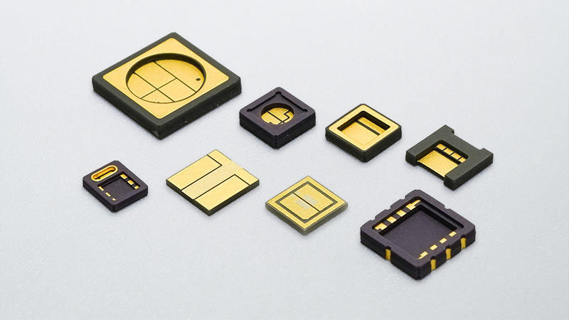
Ceramic semiconductor packages come in different structures and configurations, depending on the semiconductor device, thermal requirements, electrical connections, and operating environment.
1. Ceramic DIP
Ceramic Dual In-line Package (CDIP) is one of the traditional ceramic semiconductor package types. It features two parallel rows of pins extending from the package body and is commonly used for integrated circuits that require reliable through-hole connections.
2. Ceramic PGA
Ceramic Pin Grid Array (CPGA) uses an array of pins arranged across the bottom of the ceramic package. The large number of connection points allows CPGA packages to support semiconductor devices that require more electrical connections.
Ceramic PGAs provide good mechanical stability and thermal performance and have been used for processors, high-performance ICs, and other specialized semiconductor devices.
3. Ceramic QFP
Ceramic Quad Flat Package (CQFP) has leads extending from all four sides of the package. Unlike traditional through-hole packages, the leads are designed for surface mounting onto a PCB.
CQFP packages can provide high pin counts while maintaining a relatively compact form factor. Ceramic versions are used when the device requires the environmental and thermal advantages of ceramic materials.
4. Ceramic BGA
Ceramic Ball Grid Array (CBGA) uses an array of solder balls on the bottom of the package instead of conventional external leads. This structure allows a large number of electrical connections to be arranged in a relatively small package area.
CBGA packages can provide good electrical performance, mechanical reliability, and thermal characteristics. They are used in high-performance processors, networking devices, aerospace electronics, and other demanding applications.
5. Hermetic Ceramic Packages
Hermetic ceramic packages are designed to create a sealed enclosure around the semiconductor device. Ceramic materials are combined with metal lids, seals, and electrical feedthroughs to prevent moisture, gases, and contaminants from entering the package.
Hermetic ceramic packaging is particularly important for applications where long-term reliability is critical, such as military, aerospace, medical, and high-reliability industrial electronics.
6. Ceramic Chip Carriers
Ceramic chip carriers provide a compact package structure for integrated circuits and other semiconductor devices. They can be designed with leads or contact structures around the package and are suitable for surface-mount applications.
|
Package Type |
Main Structure |
Typical Characteristics |
Applications |
|
Ceramic DIP (CDIP) |
Two rows of pins |
Through-hole, robust, reliable |
Military, industrial, aerospace |
|
Ceramic PGA (CPGA) |
Pin array |
High connection density |
Processors, specialized ICs |
|
Ceramic QFP (CQFP) |
Leads on four sides |
Surface mount, high pin count |
Industrial and high-reliability ICs |
|
Ceramic BGA (CBGA) |
Solder ball array |
High I/O density, compact |
Processors, networking, aerospace |
|
Hermetic Ceramic Package |
Sealed ceramic enclosure |
Excellent environmental protection |
Military, aerospace, medical |
|
Ceramic Chip Carrier |
Compact ceramic package |
Thermal and mechanical stability |
Specialized ICs and electronics |
What Types of Chips Use Ceramic Packages?
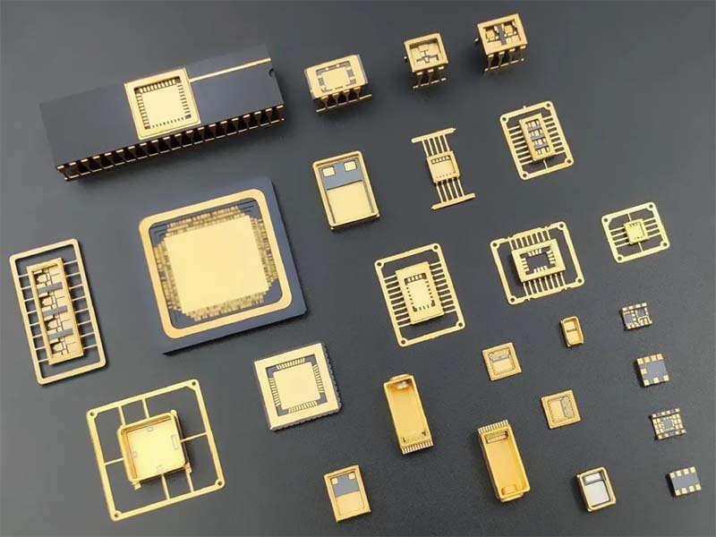
Ceramic packaging is widely used in applications that require high reliability, thermal stability, and resistance to harsh environments. It is commonly found in military-grade chips, aerospace electronics, automotive systems, industrial equipment, high-power electronics, and telecommunications. In particular, military-grade chips often use ceramic packages because they need to maintain stable performance under extreme temperatures, vibration, humidity, and other demanding operating conditions.
Ceramic Packaging Semiconductor Applications
1. Power Semiconductors
Ceramic packaging is widely applied in IGBT, SiC MOSFET, GaN HEMT and high-power diode modules. Adopting high thermal conductivity AlN and Al₂O₃ ceramic substrates, it efficiently dissipates heat under high current and high voltage operating conditions, serving core scenarios such as new energy vehicles, power grid inverters, industrial motor drives and energy storage systems.
2. RF & Microwave / Millimeter-Wave Devices
It is commonly used for RF power amplifiers, filters, switches and radar transceivers. LTCC multi-layer ceramic packaging can integrate resistors, capacitors and transmission lines inside substrates, meeting the high-performance requirements of 5G/6G base stations, satellite communication and aerospace radar equipment.
3. Optoelectronic & Photonic Chips
This packaging method applies to laser diodes, photodetectors, optical transceivers and MEMS optical switches. Its excellent hermetic performance isolates moisture and gas pollution, stabilizing optical device performance for data center optical modules, optical fiber communication and automotive LiDAR systems.
4. High-Reliability Aerospace & Military Components
Ceramic packaging is adopted for aerospace control chips, inertial sensors and high-temperature ICs. It can withstand extreme temperature changes, vacuum environments, radiation interference and mechanical shock, ensuring stable operation of core electronic equipment for satellites, aircraft avionics and military missile systems.
5. MEMS & Sensors
It is suitable for pressure sensors, inertial accelerometers, gyroscopes and gas sensors. The ceramic packaging structure protects fragile microelectronic microstructures and maintains long-term stable sensing performance, which is widely used in automotive safety systems, industrial monitoring and medical sensing equipment.
6. High-Speed & High-Temperature ICs
Applied to high-performance computing chips, storage memory and high-temperature logic ICs, ceramic packaging features low outgassing and excellent dimensional stability at high temperatures, adapting to harsh working conditions of oil exploration electronics and industrial high-temperature control equipment.
7. Medical Electronic Devices
It serves implantable medical chips and medical diagnostic sensors. The biocompatible hermetic ceramic structure effectively isolates core chips from body fluid corrosion, ensuring the safety and long-term reliability of implanted medical electronic devices.
Future of Ceramic Packaging Chips Market
The future of the ceramic packaging chips market will be shaped by the increasing performance, power density, and reliability requirements of advanced semiconductor devices.
- Growing Demand for High-Reliability Semiconductors
One of the most important drivers for ceramic packaging is the growing demand for semiconductor devices that can operate reliably under extreme conditions. Military-grade chips, aerospace electronics, space systems, automotive electronics, and industrial equipment often face high temperatures, thermal cycling, vibration, humidity, radiation, and other environmental stresses.
- Thermal Management Will Become More Important
As semiconductor power density increases, heat dissipation is becoming one of the major challenges in advanced electronics. Ceramic materials such as aluminum nitride (AlN) offer high thermal conductivity combined with excellent electrical insulation, making them attractive for high-power and high-temperature applications.
Future ceramic packaging technologies are therefore likely to focus increasingly on thermal resistance reduction, improved heat spreading, and better integration between the semiconductor die and package. This is particularly relevant to power semiconductors, RF devices, high-performance computing, and other applications where thermal performance directly affects device reliability.
- Advanced Ceramic Materials and Package for Semiconductor Designs
Future development will not depend only on conventional alumina-based packages. Different ceramic materials offer different combinations of thermal conductivity, dielectric properties, mechanical strength, and manufacturing cost.
For example, alumina (Al₂O₃) remains widely used because of its electrical insulation and established manufacturing processes, while AlN is attractive for applications requiring higher thermal conductivity. Continued development of ceramic substrates, multilayer structures, metallization technologies, and hermetic sealing methods could further expand the role of ceramic packaging.
- Cost Remains a Key Challenge
Despite its technical advantages, ceramic packaging faces an important limitation: cost. Ceramic materials and manufacturing processes can be more expensive and complex than conventional plastic semiconductor packaging. Ceramic can also be more brittle, which creates additional challenges in handling and package design.
Therefore, ceramic packaging is unlikely to replace low-cost plastic packaging across the entire semiconductor industry. Instead, its future growth is more likely to concentrate on high-value, high-reliability, high-temperature, and high-power applications where its performance advantages justify the additional cost.
The Best Ceramic-Packaged & Military-Grade Chips Supplier
For applications requiring high reliability, stable electrical performance, and resistance to demanding operating conditions, ceramic-packaged semiconductor devices remain an important choice. The following selection includes a range of analog ICs, operational amplifiers, data converters, interface ICs, switches, voltage regulators, and other high-reliability components available in ceramic packages. Many of these devices feature ceramic or hermetic package options and are designed for demanding industrial, aerospace, military, and other specialized applications.
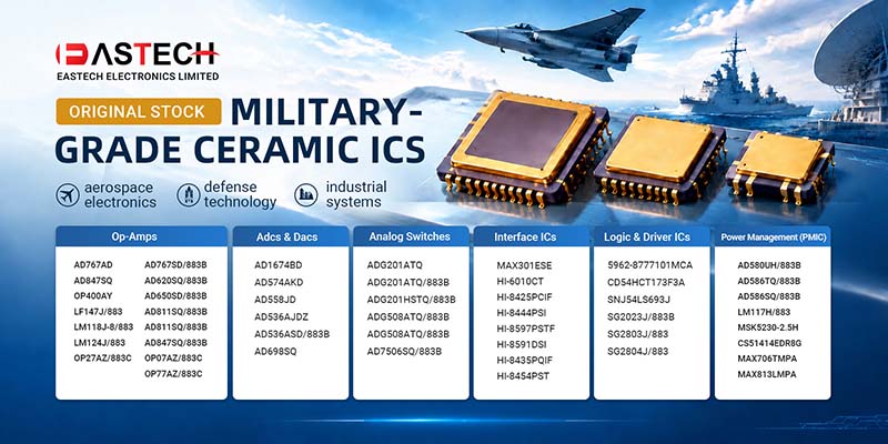
From Analog Devices (ADI), Texas Instruments (TI), Maxim Integrated, Microchip Technology, Linear Technology, Device Engineering Incorporated, Data Device Corporation, Holt Integrated Circuits, and other leading semiconductor manufacturers, we can help source a wide range of rare ceramic-packaged chips. Whether you are looking for discontinued components, military-grade ceramic ICs, or specific ceramic package variants. Submit your required part numbers or BOM to discuss sourcing options, availability and suitable alternatives for difficult-to-find ceramic-packaged components
|
AD1674BD |
7705201EA (ADG508ATQ/883B) |
CS51414EDR8G |
|
AD558JD |
5962-8859301MPA (OP400AZ/883C) |
PC817C |
|
AD574AKD |
OP07AZ/883C |
SG2003J/883B |
|
AD536AJDZ |
OP27AZ/883C |
SG2023J/883B (CDIP16) |
|
AD536ASD/883B |
5962-8773802PA (OP77AZ/883C) |
SG2803J/883B |
|
AD580UH/883B |
OP400AY |
SG2804J/883 |
|
5962-8982401PA (AD586SQ/883B) |
5962-8777101MCA |
|
|
AD586TQ/883B |
LF147J/883 |
HI-8425PCIF |
|
AD620SQ/883B |
LM117H/883 |
HI-8444PSI |
|
AD650SD/883B |
LM124J/883 |
HI-8597PSTF |
|
AD698SQ |
CD54HCT173F3A (5962-8875901EA) |
HI-8591DSI |
|
AD7506SQ/883B |
SNJ54LS693J |
HI-8435PQIF |
|
AD767AD |
LM118J-8/883 |
HI-8454PST |
|
AD767SD/883B |
MAX232AMJE/883B |
|
|
AD7802SQ-1 |
MAX706TMPA |
ADG201ATQ/883B |
|
AD811SQ/883B |
MAX301ESE |
ADG201HSTQ/883B (5962-8671603EA) |
|
5962-9313101MPA (AD811SQ/883B) |
MAX813LMPA |
ADG508ATQ/883B |
|
AD847SQ |
AD847SQ/883B |
MSK5230-2.5H |
Summary, semiconductor packaging plays an important role in determining the thermal, mechanical, and electrical characteristics of an integrated circuit, while also protecting the device during operation. Ceramic packaging offers excellent thermal stability, mechanical strength, and environmental resistance, making it well suited for demanding conditions. These properties support a wide range of ceramic packaging semiconductor applications, particularly in aerospace, defense, industrial, and military high-reliability electronic systems.
Related information
- 2026.09.13 What is SMD Resistor?
- 2026.09.06 What is Bus Interface IC?
- 2026.08.30 How to Select Supercapacitor?
- 2026.08.23 What is Aluminium Electrolytic Capacitor?