

Available 24/7 at
+86 13632816717

What is an Integrated Circuit Package?
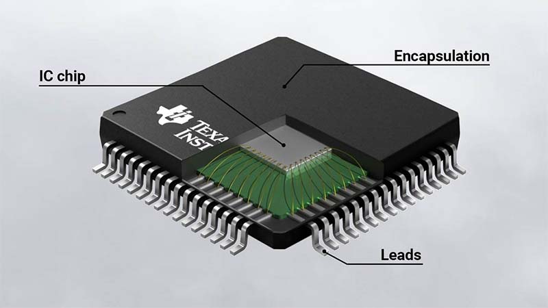
What is an integrated circuit package? An integrated circuit package (IC package) is the process of protecting, interconnecting, supporting, and providing external electrical connections for a semiconductor chip that has been fabricated on a wafer. Different electronic components package types are designed to meet varying requirements for size, thermal management, and electrical connectivity. From traditional through-hole packages to modern surface-mount designs, the choice of package affects not only the chip'
 s protection and integration into circuits but also the overall efficiency and performance of the electronic system.

Why is Integrated Circuit Packaging Important?
Integrated circuit (IC) packaging is not only a crucial final step in the chip manufacturing process but also serves as the key bridge connecting the internal circuits of a chip to external systems.
- Physical Protection: Shields the fragile bare chip from moisture, dust, mechanical stress, electrostatic discharge, and environmental damage.
- Electrical Connection: Routes the chip's internal circuitry to pins or pads, enabling signal and power connections with the PCB and external circuits.
- Heat Dissipation: Conducts and disperses the heat generated during chip operation, ensuring stable performance and preventing thermal failure.
- Signal Support: Provides electrical shielding, minimizes interference, and maintains signal integrity.
- Standardized Assembly: Establishes uniform sizes and mounting formats for easier soldering, testing, surface-mounting, and final product assembly.
- Performance and Reliability Assurance: Enhances chip lifespan, stability, and yield, making it an essential step for mass production and practical applications.
The Most Common Integrated Circuit Packaging Types
1. Classification by Pin Configuration
Through-Hole Packages
Type: DIP (Dual In-line Package)
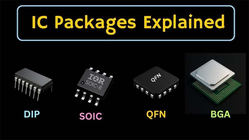
Pins extend vertically from both sides of the package and pass through holes on the PCB for soldering. This method is simple, cost-effective, and convenient for manual soldering and repair. It is commonly used in early electronic devices, educational boards, and low-pin-count general-purpose chips. The main drawbacks are large size and low integration density.
Surface-Mount Technology Packages (SMD / SMT)
Types: SOP, SOIC, QFP, QFN, BGA
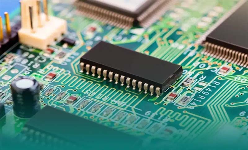
Currently the mainstream packaging type in the semiconductor industry, these packages do not require holes through the PCB. They are directly soldered onto the board surface, offering advantages such as small size, light weight, high integration density, and excellent electrical performance. They are suitable for automated pick-and-place assembly and cover most consumer electronics, industrial electronics, and communication equipment.
2. Classification by Structure and Pin Distribution
Dual In-line Packages: DIP, SOP, SOIC, TSOP
In this type of package, pins are evenly distributed along both sides of the package body. The structure is regular, and the design and manufacturing processes are mature. This classic form of IC packaging is commonly used in early and entry-level integrated circuits, including DIP, SOP, SOIC, and TSOP.
(1) DIP (Dual In-line Package)
Features: A through-hole dual in-line package with pins extending vertically downward from both sides. It has wide pin spacing and high mechanical strength, supporting manual soldering and rework. Its simple structure ensures extremely low production cost and strong resistance to environmental interference. However, its large size and limited pin count make it unsuitable for high-density circuits.
Industry Applications: Educational development boards, legacy industrial control equipment, basic appliance control chips, low-pin-count logic chips, and low-power power management chips.
(2) SOP / SOIC (Small Outline Package / Small Outline Integrated Circuit)
Features: Surface-mount dual in-line packages with gull-wing pins extending outward from both sides. They are much smaller and thinner than DIP, suitable for automated pick-and-place assembly, with high soldering yield, controllable cost, and superior electrical performance compared to DIP. SOIC is a more precise variant of SOP, with smaller pin pitch.
Industry Applications: General-purpose analog chips, small-capacity memory chips, consumer electronic peripherals, basic automotive electronic modules, and power driver chips.
(3) TSOP (Thin Small Outline Package)
Features: An ultra-thin surface-mount dual in-line package. Based on the SOP design, TSOP further reduces package thickness and pin pitch, resulting in a more compact form factor. It exhibits lower parasitic inductance and capacitance, better high-frequency performance, balanced heat dissipation, and strong reliability in pin soldering.
Industry Applications: Widely used for memory modules, Flash memory, SRAM, and other types of storage chips, making it a classic package for storage devices.
Quad-Side Pin Packages
QFP (Quad Flat Package)
Features: Pins extend from all four sides in a gull-wing shape. Pin layout is regular, and the number of pins can be high, with precise pitch control to meet multi-pin chip interconnection requirements. PCB routing is relatively easy, mass production processes are mature, and heat dissipation and signal stability are moderate. However, at high pin counts, pins can deform easily, and soldering precision requirements increase.
Industry Applications: Microcontrollers (MCUs), application-specific ASICs, mid-to-low-end processors, communication interface chips, industrial control modules, and conventional image-processing chips.
Quad-Side Leadless / Pad Array Packages
(1) QFN (Quad Flat No-leads Package)
Features: No exposed pins around the package; peripheral solder pads and a large central thermal pad are located on the bottom. Extremely thin and compact, taking up minimal PCB space. Low parasitic parameters, low high-frequency signal loss, superior heat dissipation compared to QFP and SOP, and strong soldering reliability.
Industry Applications: Smartphones, IoT devices, wearable electronics, automotive electronics, RF modules, portable medical devices, and high-density small circuits.
(2) LCC (Leadless Chip Carrier)
Features: Fully sealed, leadless package with pads on all four sides, often made of ceramic. High temperature and moisture resistance, extremely high reliability. The bottom has recessed pads for good electrical shielding, suitable for harsh operating conditions. Higher cost than QFN.
Industry Applications: Military electronics, aerospace devices, high-end automotive electronic controls, industrial high-temperature and high-voltage scenarios, and high-reliability communication modules.
Bottom Solder Ball Array Packages
BGA, FBGA, CSP (Chip-Scale Packages)
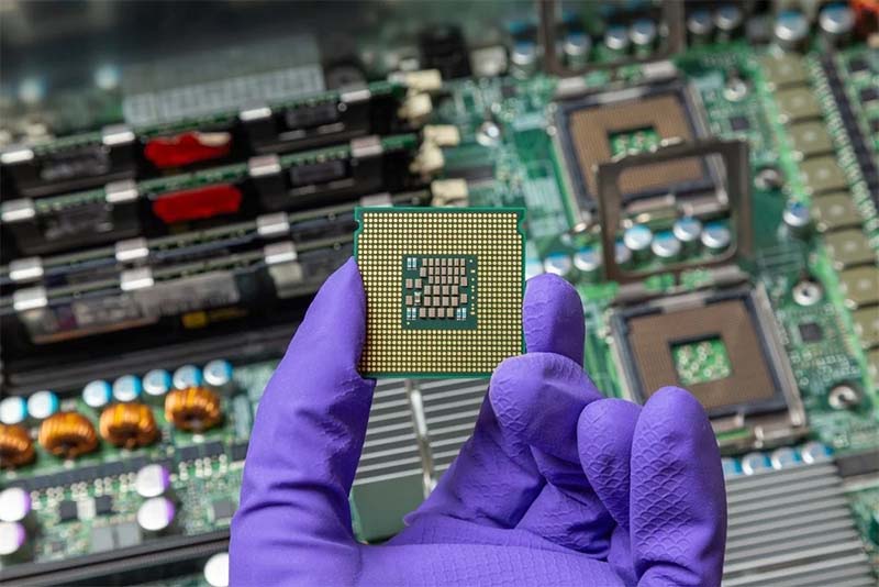
These packages eliminate traditional pins, using solder balls evenly distributed on the bottom for electrical interconnection. They offer extremely high pin density and excellent electrical performance, making them the preferred choice for high-end, high-performance chips.
(1) BGA (Ball Grid Array)
Features: Solder balls are evenly distributed on the bottom of the package. Short electrical paths reduce signal loss, provide strong resistance to electromagnetic interference, and allow efficient heat dissipation. BGAs can handle high current and high-speed signals, with far more pins than QFP, solving multi-pin packaging challenges. However, post-soldering rework is difficult.
(2) FBGA (Fine-pitch Ball Grid Array)
Features: An upgraded version of BGA with smaller ball pitch and higher density. Package size is further reduced, with a thin form factor. Electrical performance and heat dissipation are optimized simultaneously, providing more stable high-speed signal transmission.
(3) CSP (Chip-Scale Package)
Features: Ultra-compact solder-ball array package with a size nearly identical to the bare chip. One of the smallest and most highly integrated packaging types available. Extremely short interconnects, very low power consumption, fast signal transmission, and very high manufacturing precision requirements.
3. Classification by Package Material
Plastic Packages: Low cost and the most widely used.
Ceramic Packages: High temperature resistance and high reliability; commonly used in military and aerospace applications.
Metal Packages: Excellent shielding and heat dissipation; often used for high-frequency and high-power devices.
4. Classification by Integration Level and Advanced Packaging
- Single-Chip Package: One chip per package.
- Multi-Chip Package (MCP): Multiple chips of the same type are integrated into a single package to increase capacity and performance. Commonly used in high-capacity memory devices. MCP processes are simpler compared to SiP.
- System-in-Package (SiP): Integrates chips with different functions (e.g., main control, memory, sensors, RF chips) into a single package, providing complete system functionality. SiP increases integration without changing chip manufacturing processes and is widely used in 5G, IoT, and smart devices.
- 3D Stacking Package: Uses TSV (Through-Silicon Via) technology to vertically stack multiple chips, greatly reducing interconnect distance, increasing transmission speed, lowering power consumption, and further enhancing integration. Common in high-end memory, AI chips, and high-performance computing chips. 3D stacking is a core trend in future high-end chip packaging.
How are Semiconductor Chips Packaged?
Packaging an integrated circuit (IC) is the process of turning a fragile silicon chip into a durable, usable electronic component. It protects the chip, provides electrical connections, and helps manage heat.
1. Wafer Dicing (Cutting the Chips)
ICs are first fabricated on a silicon wafer, which is then precisely cut into individual dies (chips) using a saw or laser.
2. Die Attach (Mounting the Chip)
Each die is securely attached to a package substrate or lead frame using materials such as epoxy adhesive, solder, or sintered silver to ensure mechanical stability and efficient heat conduction.
3. Wire Bonding / Flip-Chip Connection
Electrical connections between the die and the package are established either through wire bonding, where thin gold or copper wires connect pads to leads, or through flip-chip technology, where the die is flipped and connected via solder bumps to form reliable electrical pathways.
4. Encapsulation (Molding the Package)
The assembled chip is enclosed in a protective material, typically epoxy resin for plastic packages or ceramic/metal for high-reliability applications, to safeguard it from moisture, dust, and mechanical damage.
5. Lead Formation & Plating
External connections are finalized by trimming and bending pins for packages like DIP and QFP or adding solder balls for BGA packages, with leads often plated in tin, gold, or silver to enhance conductivity and solderability.
6. Testing & Inspection
Each packaged IC undergoes rigorous electrical testing and visual or mechanical inspection to verify functionality and performance, ensuring that any defective units are identified and removed.
7. Marking & Final Packaging
The finished chips are marked with essential information such as part number, brand, and date code, and then packaged in formats like tape and reel, trays, or tubes for shipping and assembly.
What Materials are used for Integrated Circuit Packages?
Integrated circuits rely not only on advanced chip design but also on packaging technology to ensure performance and reliability. At the heart of packaging is the selection and combination of materials, which work together to provide protection, connectivity, and heat dissipation, forming a stable and efficient chip structure.
1. Package Body Materials
Used to encapsulate the chip, providing mechanical protection and environmental isolation.
Epoxy Molding Compound (EMC): Low cost, widely used.
Ceramic Materials (e.g., Alumina): High temperature resistance, high reliability.
Metal Materials (e.g., Kovar): Used for hermetic sealing.
2. Lead Frame / Substrate Materials
Used to support the chip and establish internal and external electrical connections.
Copper and Copper Alloys: Excellent electrical and thermal conductivity.
42 Alloy (Fe-Ni): Matches the thermal expansion of silicon chips.
Organic Substrates (BT resin, FR-4): Commonly used in BGA, CSP, and other packages.
Surface Plating (Gold/Silver/Tin): Enhances conductivity and oxidation resistance.
3. Die Attach Materials
Used to fix the chip onto the substrate or lead frame, while assisting in heat dissipation.
Epoxy Adhesives (often silver-filled): Provide both bonding and thermal conductivity.
Solder (e.g., SnAgCu): Suitable for high-temperature or high-power devices.
Sintered Silver: High thermal conductivity for high-reliability applications.
4. Bonding Materials
Used to establish electrical connections between the chip and the package.
Gold Wire (Au): High reliability and corrosion resistance.
Copper Wire (Cu): Low cost and widely used.
Aluminum Wire (Al): Commonly used in power devices.
5. Thermal Management Materials
Used to conduct heat generated by chip operation, ensuring stable performance.
Thermal Interface Materials (TIMs): Thermal grease or adhesives.
Phase Change Materials (PCM).
Metal Heat Sinks or Thermal Spreaders: Copper or aluminum components for enhanced heat dissipation.
6. External Connection Materials (Leads / Interconnects)
Used to achieve electrical and mechanical connections between the package and the PCB.
Solder (e.g., Sn-Ag-Cu): For solder balls and bump connections.
Copper Pins / Pads: Basic conductive structures.
Surface Plating (Gold / Silver / Tin): Improves soldering reliability.
Integrated circuit packaging is the critical process that transforms fragile silicon chips into stable, usable electronic components. Package body materials protect the chip, lead frames and bonding materials provide electrical connections, thermal management materials ensure efficient heat dissipation, and reliable external interconnect structures complete the package. Each step directly impacts the IC's performance and reliability. Different packaging types and application scenarios use different combinations of materials to balance cost, performance, and durability. Understanding these materials and their functions not only helps grasp the principles of IC packaging but also provides valuable guidance for component selection and procurement.
If you have any questions about IC packaging, consider consulting with professional and reliable chip and integrated circuit suppliers, as they can often provide more targeted solutions. As a trusted electronic component partner, Eastech is committed to providing customers with a stable chip supply and efficient procurement support, helping products achieve comprehensive improvements in performance and reliability.
Related information
- 2026.09.06 What is Bus Interface IC?

- 2026.08.30 How to Select Supercapacitor?
- 2026.08.23 What is Aluminium Electrolytic Capacitor?
- 2026.08.16 What are BJT and MOSFET Transistors?