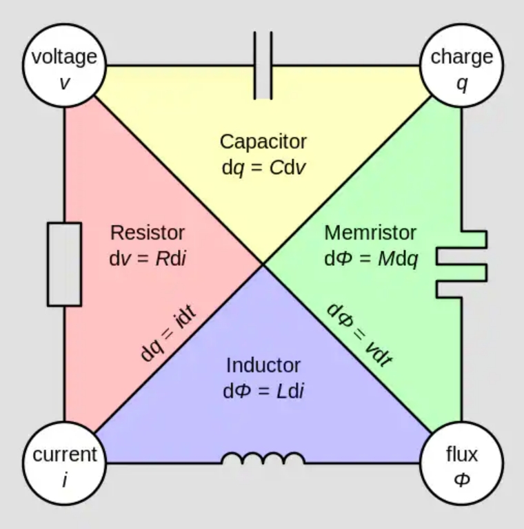
Memristors—devices that “remember” their resistive state after the device is turned off—could be used not only as digital memory but also as building blocks for future neuromorphic computers. However, building a device that meets large-scale manufacturability and cost-effectiveness requirements has been challenging.

One promising route brings memristors into two dimensions, using atomically thin layers to enable faster switching and scalability. Now, researchers at the University of Rochester have figured out how to strain a specific 2D memristor so that it has the fastest switching speeds and lowest operating energy of any such 2D device.
The resistance inside these memristors is controlled by a phase change mechanism. Normal phase change memory works like this: a glassy material (usually a chalcogenide) is sandwiched between two contacts. Electric current passing through the glass can change its phase between a low-resistance crystalline state and a high-resistance amorphous state. This allows for large differences in resistivity between the two states, making them attractive for memory devices. But introducing this behavior into a two-dimensional film can cause problems—defects in the glass may inhibit consistent phase transitions and increase the necessary operating voltage.
Back in 2019, researchers at Purdue University and the National Institute of Standards and Technology proposed a new phase-change mechanism that is more suitable for thin films. They used molybdenum ditelluride, a transition metal dichalcogenide-like material capable of arranging itself into several different phases. For their memristor, the team switched a two-dimensional film of molybdenum ditelluride between a high-resistance semiconductor phase and a low-resistance semi-metallic phase. This turns out to be a more robust phase change in compact devices, but the switching voltage required is quite high - more than one volt per phase change. The switching energy of each switch is three femtojoules – quite high for a device of this type.
The Rochester team added a controlled amount of strain to the 2D film, forcing it to teeter on the edge between two stages. This reduces switching speed and switching energy by several orders of magnitude – only 0.1 volts and 120 ajoules are required to switch. Additionally, the resistance ratio between the two states is 10 8 , the highest among all 2D memristors.
What’s exciting about this approach is that they’re using engineered strains. Rather than adding steps to the manufacturing process, they use existing technology to their advantage. Contacts naturally develop some stress as they are deposited and patterned. When the device is constructed, stress from the contacts is released into the molybdenum ditelluride, straining it in both directions. By precisely controlling the thickness and angle of the contacts, the team was able to engineer the precise amount and direction of strain that allows the device to function optimally.
“Whenever you make these devices,” said Stephen Wu, an assistant professor at the University of Rochester and the lead researcher on the results, “you build up stress and strain on the wafer anyway, so you either zero out everything, or you You can just use it and it will really enhance your device.”
There are several other metrics that need to catch up before these devices are ready for prime time. The device's state was retained for just over a day and performance degraded after hundreds of switches. Wu said the team is working on miniaturizing the memristor, and preliminary results show that performance will only improve as the memristor shrinks. They are also looking at retention and robustness. As this is the first demonstration of the device, further engineering is required. But, Wu said, "These are common challenges in the field, and we may be able to draw on existing ideas to overcome these obstacles."


